 how-to
How to Spot Poor Soldering: 7 Visual Signs
Table of Contents
- Why Spotting Poor Solder Joints Early Matters
- Cold Solder Joint Symptoms: The 7 Visual Signs of Poor Soldering
- Tools for Inspecting Solder Connections
- Solder Joint Inspection Best Practices for Through-Hole and Surface Mount
- How to Fix a Poor Solder Joint: Desoldering and Reflowing
- Conclusion: Trust Your Inspection Before You Power Up
- Frequently Asked Questions
Last Updated: September 9, 2026
Why Spotting Poor Solder Joints Early Matters
A single poor solder joint can turn a working circuit into an intermittent nightmare that resists every troubleshooting attempt. Learning how to spot poor soldering before you power up saves hours of frustration and protects expensive components from thermal damage caused by repeated rework. The stakes are even higher in equipment that carries liquids or operates under vibration, where a fractured joint can fail catastrophically.
At Steven StillZ LLC, we build hand-crafted copper stills where every joint must hold up under heat and pressure. A cold solder joint is a connection where the solder failed to fully melt and wet both surfaces, leaving a mechanically weak and electrically unreliable bond (sciencedirect.com). Most defective joints reveal themselves through visual cues you can learn to read with practice and the right tools.
Below, we walk through the seven visual signs of poor soldering, the tools that make inspection reliable, and the exact steps to rework a bad joint.
Cold Solder Joint Symptoms: The 7 Visual Signs of Poor Soldering
The fastest way to spot poor soldering is to compare the suspect joint against a known-good reference under bright light. A proper solder joint has a smooth, shiny, concave fillet that wets the pad and the component lead evenly, with no visible boundaries between solder and metal. Anything that deviates deserves a closer look.
Know Your Alloy First: Leaded vs. Lead-Free Appearance
Before judging a joint as defective, you must know which solder alloy was used. This single factor changes what "good" looks like and prevents you from flagging a healthy joint as a failure.
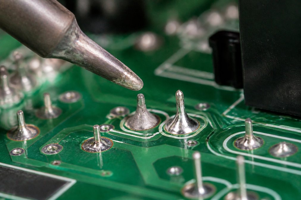
Leaded solder (63/37 tin-lead or 60/40): This alloy solidifies with a bright, mirror-like, almost wet-looking finish. The surface is smooth and highly reflective, and the fillet has a distinct concave curve. A dull, frosted, or matte surface on leaded solder is a strong indicator of a cold joint or insufficient heat.
Lead-free solder (SAC305: 96.5% tin, 3% silver, 0.5% copper): This is the default alloy for most consumer electronics manufactured after the Restriction of Hazardous Substances (RoHS) Directive took effect in July 2006. Lead-free solder does not look like leaded solder. A healthy SAC305 joint has a satin or slightly matte finish that is noticeably less shiny than its leaded counterpart, often appearing grainy at the microscopic level even when perfect. The fillet is also less pronounced and may look slightly more flat or lumpy.
Applying the "bright and shiny" rule to a lead-free joint will misdiagnose a perfectly good connection as defective. The correct test for lead-free is a uniform, consistent satin texture with no frosty, chalky, or crystalline patches. A truly cold lead-free joint looks dull, porous, and often has a rough, crumbly surface that flakes under light pressure from a probe.
Dull, Grainy Surface vs. Bright Finish
The most obvious indicator is surface texture, but you must interpret it through the alloy lens above. A healthy leaded joint has a bright, almost mirror-like finish, while a cold joint appears dull, frosted, or grainy, resembling oxidized pewter. For lead-free solder, the healthy baseline is a uniform satin sheen, and the defect signature is a patchy, non-uniform dullness with visible crystalline structure.
That dull finish signals insufficient heat during soldering, meaning the flux did not fully activate and the solder did not properly alloy with the surfaces. A grainy texture points to the solder solidifying while still semi-molten, often because the iron was removed too early or the joint moved during cooling. Either way, the joint integrity is already compromised regardless of how it tests electrically right now.
Concave Fillet, Excessive Solder, and Solder Bridges
Look at the shape of the solder where it meets the pad. A correct fillet is concave, curving inward like a smooth bowl between the lead and the pad, indicating proper wetting and a strong metallurgical bond. This holds true for both leaded and lead-free alloys, though the concavity is shallower with lead-free due to its higher surface tension.
A convex, bulging joint shaped like a dome tells a different story: the solder beaded up on the surface instead of wetting it, which happens when the pad was dirty, oxidized, or not hot enough. Excessive solder that obscures the component lead entirely makes inspection impossible. A solder bridge, where excess solder spans two adjacent pads or leads, creates a short circuit that can destroy components the moment you apply power.
Cracks, Fractures, and Solder Balling
Cracks and fractures in a solder joint are the most serious visual defect because they indicate mechanical stress or thermal shock after soldering. Hairline cracks often appear at the interface between the solder and the component lead, nearly invisible without magnification. On lead-free joints, look for "fillet lifting," where the solder separates from the pad or lead in a clean, often shiny break indicating stress during cooling.
Solder balling, where tiny spheres of solder scatter around the joint, signals contaminated surfaces or solder that oxidized during the process. These balls can roll between traces and cause intermittent shorts that are maddening to diagnose later. A fractured joint may pass a continuity test when the crack is closed under no stress, then fail when the board flexes or heats up, which is why visual inspection matters even when your multimeter says everything is fine.
Tools for Inspecting Solder Connections
You cannot reliably spot poor soldering with the naked eye alone, so a basic inspection kit is essential. A 10x loupe or jeweler's eyepiece reveals surface texture, cracks, and wetting quality that looks acceptable at arm's length.
For surface mount work, a stereo microscope or digital USB microscope with 20x to 50x magnification makes the difference between guessing and knowing. Good lighting matters as much as magnification: an adjustable LED work lamp at a low angle casts shadows that expose dull finishes and hairline fractures. A multimeter with continuity and resistance modes completes the kit, giving you a non-visual check when the joint looks marginal.
Solder Joint Inspection Best Practices for Through-Hole and Surface Mount
Through-hole and surface mount joints demand different inspection priorities, and the tools and techniques that work for one often fail for the other. Understanding the distinct failure modes of each package type is the difference between catching a defect and shipping a latent failure.
Through-Hole Inspection: The Barrel Is the Weak Point
For through-hole work, confirm the solder fills the plated hole completely and forms a fillet on both sides of the board, not just the side where you applied the iron. A common mistake is judging a through-hole joint only from the top, when the defect hides on the barrel or the bottom fillet.
The top-side fillet test: The solder should wet the lead and the annular ring on the component side, forming a visible concave fillet. If the solder only sits on top of the hole without wicking down the barrel, you have a classic "tombstoned" or insufficient-wetting defect that will fail under vibration.
The bottom-side fillet test: Flip the board and verify that solder has wicked through to form a fillet on the solder side. A joint that looks perfect on top but has no bottom fillet means the solder did not fully penetrate the plated through-hole, leaving a weak mechanical connection and high-resistance path. This is the single most common hidden defect in hand-soldered through-hole work.
The barrel fill test: Under magnification, look through the hole (if the lead does not fully obscure it) or use a backlight to check for complete solder fill. A properly filled barrel shows no void or gap between the lead and the plated wall. Voids reduce current-carrying capacity and create stress risers that crack under thermal cycling.
Surface Mount Inspection: Fine-Pitch Demands Different Rules
Surface mount components require checking the solder wetting along the entire visible side of the pad and verifying you have not bridged to neighboring pins. But the inspection workflow changes dramatically based on package type.
Chip components (0402, 0603, 0805): These two-terminal packages fail most often from tombstoning, where one end lifts off the pad during reflow, or from insufficient solder on one termination. Inspect both ends of the component, not just the side facing you. A proper joint shows a smooth fillet rising up the metallized end. If one end shows no fillet or the component sits at an angle, the joint is suspect.
Fine-pitch QFP and SOP packages (0.5mm to 0.65mm pitch): These require 20x to 50x magnification and a different visual test. Look for the "heel fillet", the solder that wets up the back of the lead where it meets the package body. A missing or incomplete heel fillet indicates the lead did not reach reflow temperature. Also check for solder bridges between adjacent leads, nearly invisible at arm's length but catastrophic when powered. Tilt the board under raking light to catch the glint of a bridge.
BGA and QFN packages: These have hidden solder joints under the component that you cannot see at all. Visual inspection is limited to checking for proper reflow indicators: solder balls that have collapsed and wet to the pad, visible as a slight bulge around the package edge, and the absence of solder balls that have rolled free. For QFN packages with exposed thermal pads, verify that solder has wicked up the side of the pad, indicating the thermal pad reached reflow temperature. If you suspect a BGA defect, you need X-ray inspection, which is beyond the scope of visual checks.
Lighting Geometry: The Angle Reveals the Truth
In both cases, tilt the board under your light source to catch the glint of a proper fillet versus the flat, lifeless look of a cold joint. Raking light, light coming from a low angle nearly parallel to the board surface, casts shadows that expose hairline cracks, solder balls, and incomplete wetting that overhead light hides. A simple adjustable LED task lamp positioned at 15 to 30 degrees above the board surface works better than an expensive ring light for defect detection.
Non-Visual Diagnostics: Multimeter Continuity Testing
Visual inspection catches most defects, but some joints fail only under load, so you need a non-visual confirmation method. Set your multimeter to continuity mode and probe across the joint, from the component lead to the pad or trace it connects to.
A cold solder joint often shows high resistance or an intermittent continuity reading that changes when you gently flex the board with a non-conductive probe. Compare the reading against a known-good joint on the same board to establish a baseline. This technique is especially valuable for spotting fractured joints that look passable but break electrical contact under mechanical stress or thermal cycling.
For intermittent faults that only appear under load, a more advanced technique is to measure voltage drop across the suspect joint while the circuit is powered. A healthy joint drops less than a few millivolts; a cracked or cold joint can drop 50 to 100 millivolts or more, which translates to measurable heat generation and eventual failure (peer-reviewed research). This test requires a known-good reference point and a digital multimeter with millivolt resolution, but it catches defects that visual inspection and passive continuity testing miss entirely.
How to Fix a Poor Solder Joint: Desoldering and Reflowing
When you find a defective joint, the fix is straightforward: remove the old solder completely, clean the area, and start fresh. Apply fresh flux to the joint first, then touch your soldering iron set to the proper temperature for your solder alloy to the joint and let it flow.
For a joint that simply did not wet properly, a reflow attempt with additional flux and heat sometimes saves the connection without full desoldering. If the joint shows cracks, excessive solder, or contamination, desolder it completely using braid or a vacuum pump, then clean the pad with isopropyl alcohol to remove flux residue and oxidation. Always re-tin the component lead before soldering it again, and let the joint cool without moving the component to prevent thermal shock that causes new fractures.
Conclusion: Trust Your Inspection Before You Power Up
Poor soldering hides in plain sight, but the seven visual signs dull grain, convex fillets, bridges, cracks, and stray solder balls give you everything you need to catch defects before they cause damage. Build the habit of inspecting every joint under magnification with proper lighting, and confirm suspect connections with a multimeter before you apply power.
At Steven StillZ LLC, we apply the same discipline to every still we build, using 100% lead-free silver bearing solder and rigorous water and pressure testing on every unit. That commitment to joint integrity is why our customers trust their equipment to perform leak-free batch after batch. Order Online 24/7 and experience the difference that meticulous craftsmanship makes in your final product.
Frequently Asked Questions
What is the most common visual sign of a cold solder joint?
A dull, grainy, or frosted appearance is the most common sign. A good joint has a bright, shiny finish. Poor wetting also causes the solder to ball up instead of forming a smooth concave fillet. If the joint looks chalky or has a rough texture under magnification, it likely suffered from insufficient heat or the joint moved during cooling.
What tools do I need for solder joint inspection?
A 10x to 20x jeweler's loupe or a stereo microscope is essential for spotting fine cracks. A bright, direct LED light helps reveal the difference between a shiny and a dull finish. For non-visual diagnostics, a multimeter set to continuity or resistance mode confirms whether the joint conducts electricity properly. Magnification and lighting are the two most important tools.
Can poor soldering cause equipment leaks or electrical failure?
Yes. In electrical systems, a fractured joint creates an intermittent connection that causes random failures or complete circuit loss. In copper distillation equipment, a poorly soldered seam can leak vapor or liquid under pressure. This is why rigorous water and air pressure testing after assembly is critical for leak-free performance.
How do you fix a fractured or dry solder joint?
Apply fresh flux to the joint to remove oxidation, then reheat it with a properly tinned soldering iron until the solder flows freely and forms a smooth fillet. For a truly fractured joint, remove the old solder with desoldering braid or a solder sucker first. Then re-tin the surfaces and apply fresh solder. Never just add solder on top of an old joint.